Co-optimized Materials, Processes and Layouts for Superconducting Circuit Components
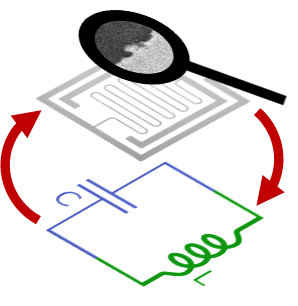
State-of-the-art superconducting qubits are composed of lithographically patterned thin films of superconducting materials on insulating substrates. In order to read out and manipulate the state of superconducting qubits they are coupled to microwave resonators. A common material choice for the planar resonator includes niobium, while the qubit structure, coupled to this resonator, is based on niobium and aluminum. The choice of the involved materials and process parameters, on which the components are based, are critical for the performance, e. g. relaxation times, of the circuits (LC-resonator connected to the qubit). For a better understanding of the circuit, the resonator can be described as LC-circuit and the qubit through an additional electronic component in state of the art electronic simulation tools. The optimization of the circuit is realized on simulation level and critical parameters are identified and provided to the manufacturing process.
Therefore, the aim of this project is to develop a digital twin for superconducting circuits that are implemented in qubit systems. The performance of superconducting qubits is limited by energy dissipation and low coherence times. In order to study design specific decay mechanisms we intend to use an electrical equivalent LC-model, including the transmon as a microcell, to study the effects of different materials, various physical layouts, as well as the electrical, frequency dependent properties of the LC control circuitry. We further extend the modeling of the LC circuits by including parametric models for the frequency dependence of the capacitor and inductors directly based on their layout shape. To this end, extensive experimental electrical characterization techniques will be employed to study the effects of various materials and layouts empirically and use regression algorithms to develop model representations.
Similarly to standardized electrical circuit modeling, we want to merge our simulation environment into widespread Design Tools and EM Simulators to allow for the design optimization on layout and schematic level. This endeavor is one of the first milestones to enhance common electronic design automation tools to become usable not only for constructing VLSI circuits, but also to become compatible with quantum devices and their corresponding transport properties to be included into the design flow.
| Name | Institute |
|---|---|
| Ioan Pop | Institute for Quantum Materials and Technology (IQMT) |
| Jasmin Aghassi | Institute of Nanotechnology (INT) |
| Gabriel Cadilha Marques | Institute of Nanotechnology (INT) |
| Haoran Duan | Institute of Nanotechnology (INT) |
| Thomas Reisinger | Institute for Quantum Materials and Technology (IQMT) |


